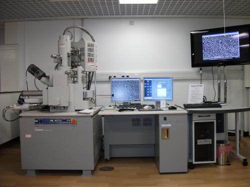
Field Emission Scanning Electron Microscope (FE-SEM)
Analysis Types:
- Morphological and topographical imaging
- Surface fractography
- Materials microstructure
- Grain size and texture analysis by electron backscattered diffraction (EBSD)
- Material composition by backscattered electron (BSE) imaging
- Elemental analysis and mapping by means of energy dispersive spectroscopy (EDS)
- Wavelength dispersive spectroscopy (WDS) for concentrations ≤500ppm or element overlaps (e.g. Mo/S)
- Variable pressure mode for non-conductive specimens – i.e. when carbon/gold coating not possible
- Scanning transmission electron microscopy (STEM) on thin films
IMPORTANT NOTE: CANCELLATIONS / SESSION USE
Bookings are not charged if cancelled up to 24h prior to the booking start time. If cancelled within 24h of booking, full fee will be charged. If during the SEM session, the user realises that they cannot use the instrument due to the condition of the samples (i.e. not correctly prepared or dried), the user will be charged for the session.
Lab: Advanced Materials Research Laboratory (AMRL) - Characterisation Laboratory
Location: James Weir Building
G1 1XJ
Owner: Advanced Materials Research Laboratory (AMRL)G1 1XJ
Contact: Advanced Materials Research Laboratory (AMRL)